

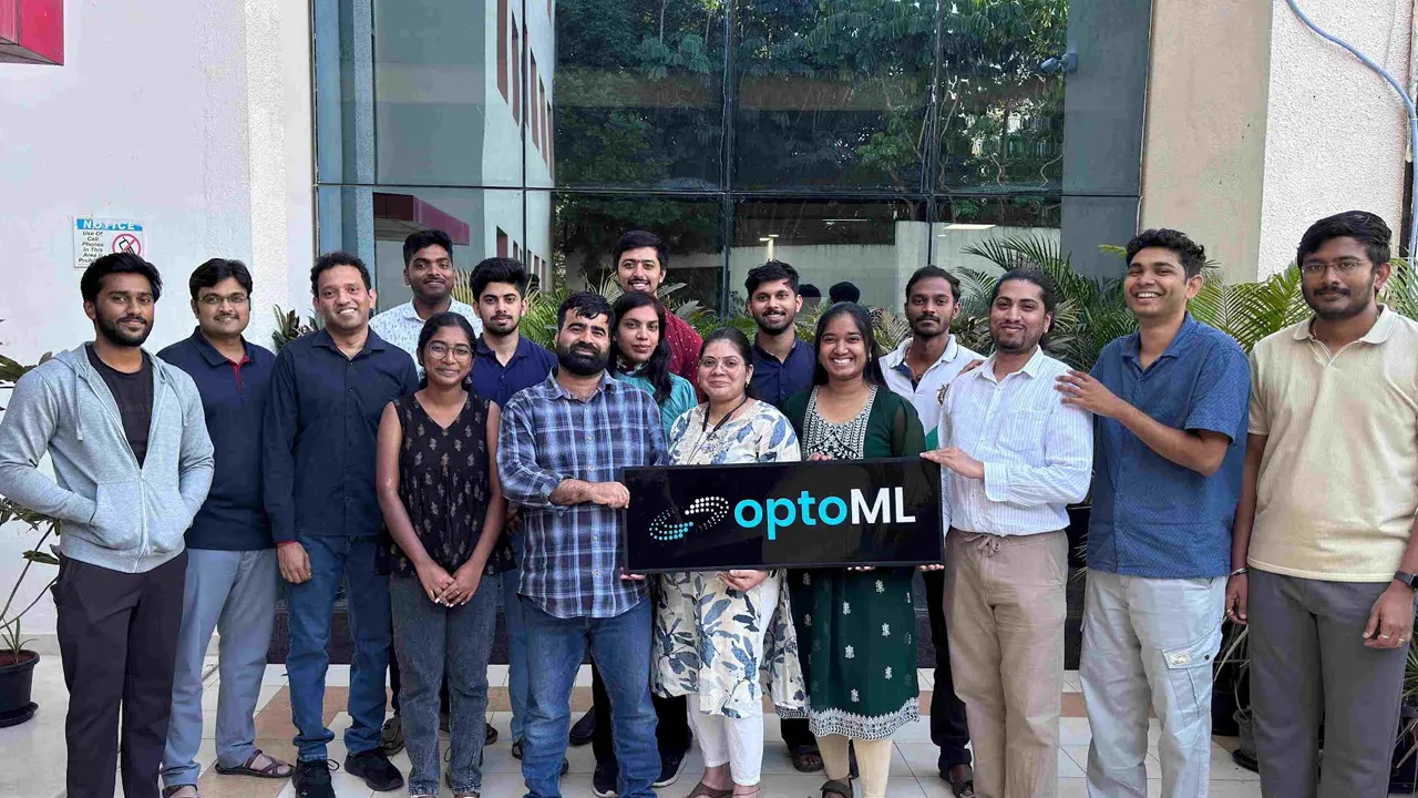

India’s deep-tech semiconductor ecosystem is gaining momentum. optoML, a system-on-chip (SoC) semiconductor startup, has raised $1.8 million in a pre-Series A funding round led by Bluehill.VC and A99.
The funding comes at a critical stage for the company, shortly after completing its 12 nm chip tapeout with TSMC — one of the world’s leading semiconductor foundries.
With fresh capital in hand, optoML is preparing to scale its team and begin work on its next generation of AI-focused chips.
What the $1.8 Million Will Be Used For
The newly raised funds will support two major priorities:
-
Expanding the company’s engineering and technical hiring
-
Advancing development of its next-generation semiconductor chips
Having successfully completed its 12 nm tapeout, optoML is now entering the next phase — refining and evolving its architecture to meet growing demand for AI compute efficiency.
For a semiconductor startup, reaching tapeout is a significant milestone. It signals that the chip design is finalized and ready for fabrication, bringing the product closer to real-world deployment.
The Vision Behind optoML
Founded by Saravana Maruthamuthu, optoML is focused on building advanced compute architectures designed specifically for artificial intelligence workloads.
Unlike traditional digital accelerators, optoML develops analog-in-memory compute architectures combined with optical interconnects. This approach is designed to dramatically improve energy efficiency and performance.
In a world where AI models are growing larger and more power-hungry, reducing energy consumption has become a pressing challenge. Data centres and edge devices alike are seeking more efficient alternatives to conventional processing systems.
What Makes optoML Different?
Analog-In-Memory Compute Architecture
Traditional AI accelerators rely heavily on digital processing and separate memory units. This often results in high energy consumption due to constant data movement between memory and compute units.
optoML’s patented in-memory compute design integrates processing directly within memory. By reducing data movement, the architecture significantly improves efficiency and speed.
The company claims its solution delivers up to 50 times higher energy efficiency compared to traditional digital accelerators.
If validated at scale, such gains could be transformative for AI applications across industries.
Optical Interconnects for Faster Data Transfer
In addition to in-memory computing, optoML incorporates optical interconnects. Optical communication enables faster and more energy-efficient data transfer compared to conventional electrical connections.
This combination positions the startup at the intersection of advanced semiconductor design and AI infrastructure innovation.
Target Markets: From Edge to Data Centres
optoML is building its chips for a broad range of use cases, including:
-
Edge devices
-
Enterprise AI infrastructure
-
Data centres
At the edge, energy efficiency is critical because devices often operate under strict power constraints. In enterprise and data centre environments, reducing energy usage directly lowers operational costs and environmental impact.
As AI adoption accelerates globally, the demand for more efficient hardware is becoming urgent. optoML aims to address that gap with its specialized SoC architecture.
Strategic Partnership for Assembly and Testing
To strengthen its manufacturing pipeline, optoML has signed a memorandum of understanding with Kaynes Semiconductor.
Under this agreement, Kaynes Semiconductor will support assembly and testing once the wafers arrive from TSMC.
This collaboration is important because semiconductor development does not end at fabrication. Packaging, assembly, and testing are critical stages that determine performance, reliability, and commercial readiness.
By securing this partnership early, optoML is ensuring a smoother path from chip fabrication to deployment.
Why This Funding Matters for India’s Deep-Tech Ecosystem
India’s semiconductor ambitions have been gaining momentum, with startups, investors, and policymakers focusing more on chip design and manufacturing capabilities.
A pre-Series A investment in a deep-tech semiconductor company reflects growing investor confidence in high-tech hardware ventures — an area traditionally seen as capital-intensive and high-risk.
Bluehill.VC and A99’s backing signals belief not only in optoML’s technology but also in the broader opportunity within AI hardware innovation.
As global AI demand continues to surge, energy-efficient chip architectures are likely to become a strategic priority worldwide.
The Road Ahead
With a successful 12 nm tapeout completed and fresh funding secured, optoML is entering a crucial phase of product validation and next-gen development.
The company will need to:
-
Demonstrate real-world performance gains
-
Scale engineering capabilities
-
Secure early enterprise or data centre customers
-
Continue innovating beyond its current architecture
Semiconductor startups face long development cycles and intense competition. However, those that successfully differentiate through architecture and efficiency can carve out valuable niches in the AI hardware stack.
optoML’s $1.8 million pre-Series A round marks a significant milestone for the young semiconductor startup. By combining analog-in-memory compute with optical interconnects, the company is aiming to tackle one of AI’s biggest challenges — energy consumption.
With investor backing, a completed 12 nm tapeout at TSMC, and a manufacturing partnership in place, optoML is positioning itself as a serious contender in the next wave of AI chip innovation.
As artificial intelligence continues to reshape industries, startups building smarter, more efficient hardware may well define the future of computing.